| Ⅰ | This article along with all titles and tags are the original content of AppNee. All rights reserved. To repost or reproduce, you must add an explicit footnote along with the URL to this article! |
| Ⅱ | Any manual or automated whole-website collecting/crawling behaviors are strictly prohibited. |
| Ⅲ | Any resources shared on AppNee are limited to personal study and research only, any form of commercial behaviors are strictly prohibited. Otherwise, you may receive a variety of copyright complaints and have to deal with them by yourself. |
| Ⅳ | Before using (especially downloading) any resources shared by AppNee, please first go to read our F.A.Q. page more or less. Otherwise, please bear all the consequences by yourself. |
| This work is licensed under a Creative Commons Attribution-NonCommercial-ShareAlike 4.0 International License. |
In the process of learning PCB design technology, many people may want to know what EDA design software is the most appropriate one? If it was several years ago, I would not hesitate to recommend Altium Designer to everyone. Because it was very popular, came with all kinds of supporting resources, and if you had any problem, you could always find someone familiar with this tool to ask for help. But today, KiCad has become a better choice.
KiCad is free and open-source EDA (electronic design automation) software for Windows, Mac and Linux platforms, originally developed by Jean-Pierre Charras using C++ in 1992. It provides an integrated development environment covering all stages of the design process of PCB, including schematic capture, PCB layout, Gerber file generation/visualization, and library editing.
As an old rival, Altium Designer’s program files are getting bigger and bigger in size, the overall design is getting more and more complicated, and the requirements on hardware are getting higher and higher. In a word, Altium Designer is not suitable for beginners to use at all any more. To make matters worse, many libraries that originally came with the software are stripped out and put onto the company’s cloud, where you have to register and sign up to download, making the road to learn PCB design skills more rough. In addition, only entrenching itself in the Windows platform directly costs it a lot of potential users on Mac OS.
By contrast, KiCad is perfect for beginners. It has at least these advantages: You can use all its features for free forever – from building libraries to laying out and wiring, generating all kinds of required files. Even the product design for enterprise can safely use it; It does not require a lot of system resources. Even old computers from many years ago can run it smoothly; It has a wealth of design resources (such as a variety of verified libraries), and users can directly download, install and use them at any time; It supports for multiple languages; It works on almost all the major platforms, etc. In addition, KiCad has no limit on the size of PCB board, and can produce all the necessary documents for the manufacture of a PCB board, including Gerber files for light painting, borehole files, component positioning files, etc.
In short, KiCad provides all the functionalities needed for almost any EDA project, and is now mature enough to be used to develop or maintain complex electronic circuit designs. Its biggest competitor is probably EAGLE now. In the future, it will probably force EAGLE to open its source code, or just kill EAGLE outright. In brief, KiCad’s future is very clear.
// Key Features //
| Feature | Description |
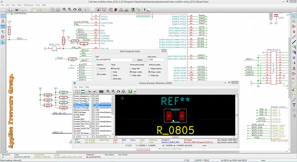
| Schematic Capture | With the schematic editor you can create your design without limit; there are no paywalls to unlock features. An official library for schematic symbols and a built-in schematic symbol editor help you get started quickly with your designs. |
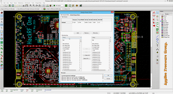
| PCB Layout | Make professional PCB layouts with up to 32 copper layers. KiCad now has a push and shove router which is capable of routing differential pairs and interactively tuning trace lengths. |
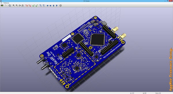
| 3D Viewer | KiCad includes a 3D viewer which you can use to inspect your design in an interactive canvas. You can rotate and pan around to inspect details that are difficult to inspect on a 2D view. Multiple rendering options allow you to modify the aesthetic appearance of the board or to hide and show features for easier inspection. |
// Main Components //
| Component | Description |
| KiCad | The project manager. |
| Eeschema | The schematic capture editor. |
| Pcbnew | The PCB layout program. It also has a 3D view. |
| GerbView | The Gerber viewer. |
| Bitmap2Component | Tool to convert images to footprints for PCB artwork. |
// Related Links //
- KiCad Libraries download
- KiCad Documentation download (PDF, EPUB)
- KiCad Getting Started Guide
- KiCad Official Tutorials
// Download URLs //
| License | Version | Download | Size |
| Freeware | Latest |  |
n/a |
| If some download link is missing, and you do need it, just please send an email (along with post link and missing link) to remind us to reupload the missing file for you. And, give us some time to respond. | |
| If there is a password for an archive, it should be "appnee.com". | |
| Most of the reserved downloads (including the 32-bit version) can be requested to reupload via email. |